Let (re)design a PCB board!

During the time at elcon a/s and Pridana Elektronik I also made some PCB-layouts using the Pads Software of Mentor Graphics. Sometimes customers ordered PCB having no data for it. The only way was to redesign the layout from the existing pcb (soldered or not).
Every layout was a challenge! The more complex the layout, the more work to do.

This and the others designs are prepared whithout any netlist. Starting from skratch, having nothing more than the PCB itself.

And btw. multilayers were not possible for redesign. Why? Try to find out the aswer by your self!


754692-518d

754692-518d

The holes

The very first step is to place the holes. There are no coordinates where the hole should be placed. Knowing the package of an electronic element it is possible to find the pitch in the database. Another way is to use a scan of the PCB, but how unprecize the scan could be, knows only one who has prepared some layouts before.

1702-391

1702-391

The Scan of a PCB

A good scan is the half way to make a board. I remember my first board, where I photographed the real PCB with my phone-camera. Based on that I designed the board and the result was horrible! Because of the collimation of the linse I got the picture streched and sqizzed in all directions, however only few tenth of milimeters, but still too much to get the propper size of board.

Using a flatbed scanner with high resolution one can achieve good results.

755045-518e

This design was a real challenge! I spend on it almost 10 working days, and when finished it showed that the board has some broken connections causing very hard to check the design on the eltest machine. First when brokens were soldered a realiable test could be executed and the design checked for mistakes.

755045-518e

The netlist

Don't dream about the netlist! Every single connection must be made by hand. The perfect way is to use the scan as a background for the connections. And this on two layers simulatenously. This part of redesign is very important for the layout, which will be created in the next step. On this step any mistake can be very costly. But I could find a reliable test to be 100% sure about my netlist.

1811-a93

A SMD-design with many LEDs on board.

1811-a93

The new layout

Having the netlist it is just a piece of cake to make the connections on the board. It's important to assign the thickness of the board and the used copper clad, width of traces, clearances, routing directions and so on.. A mistake in the settings will take much time when rerouting is needed. The thing is to put the traces as close as possible to the original layout. Here we make a copy o a PCB not an own design. However it would be faster and sometimes smarter to use the possibilities our routing program offers. But there are customers not allowing any kind of creativity.

754638-913a

The silk screen on this board was not designed, but it was recognized automatically by the software. A skilled eye can quickly see a difference comparing with drawed traces. This solution was a compromise between quality and speed.

754638-913a

plc_interface

Not a real challenge.. But still a few hours to finish the design was necessary.

plc_interface

The test

Finally we got ready our layout and it's time to check it. How one can be sure about the connections? There is an reliable electrical test, which ensures the right connections in the netlist.

Usually we use the test machine to test the boards, but this time we are testing the data. Having the original PCB we run the test-program we created from our new layout and test the board for shorts and opens. When any mistake shows up, will that mean, that the data is not OK. A short on the test-machine means we have an open in the data. And opposite. Quick reroute and the new layout is ready!

This test is a MUST to further avoid an unnecessary production of a failured PCB board, which could have some netlist errors.
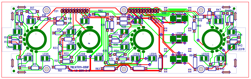
kt011

From the real board to the design..

kt011

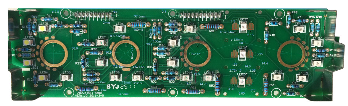
A dimmensioning of the real board is the basic when creating the proper design. Slide potentiometers, connectors and LEDs must be placed on same place as on the original board. When misplaced the components will not fit into the case.

kt011