The UCAM

CAM preparation software

https://www.ucamco.com


CAM preparation

preparing of a single PCB:

  • input gerber data and check for logical content, check if data complete
  • assign layer names, types and build up
  • check for polarities, if needed then reversing of copper layers, flatten of layers
  • create of reference netlist
  • prepare profile (closed polygon), make the rout, add break tabs, if v-cut needed, then add of 0.9mm lines
  • remove of outline on all layers, check for holes (sizes and number) and overlapping holes, check npth to copper
  • contourize of drawed power/ground areas, remove non functional pads
  • remove copper on npth holes, pad reconstruction on all layers if pads drawed (flashing)
  • DMF-check for inner and outer layers (in reference to drill and rout)
  • check for solder mask, cut and repair of solder bridges, check for silk screen, cut the silk screen to pads
  • create any additional masks if necessary: peelable, carbon, gold pads
  • add manufacturer logo, add etch compensation on all copper layers
  • create a drawing with map of holes, compare a netlist

preparing of a customer panel:

  • place the single PCB in customer panel, step up and rotate if necessary
  • create of profile and rout (round of corners 1-2mm), add tooling holes, fiducials, copper ballance
  • open for fiducials, holes in the solder masks, add manufacterer logo/date and additional text into copper/mask layer
  • make output for electrical tester (customer panel)

preparing of production panel:

  • step up the customer panel, frame is generated automaticaly
  • make output for drill, rout (obs: inner rout, nibble, compensation), check cnc-file for errors
  • make the output for electrical tester, make output for electrical tester (production panel)
  • make the AOI data, remove balancing copper

UCAM - what is it? And why I did learn it?

UCAM is a tools used on preparation for production of Printed Circuit Boards (PCB). 
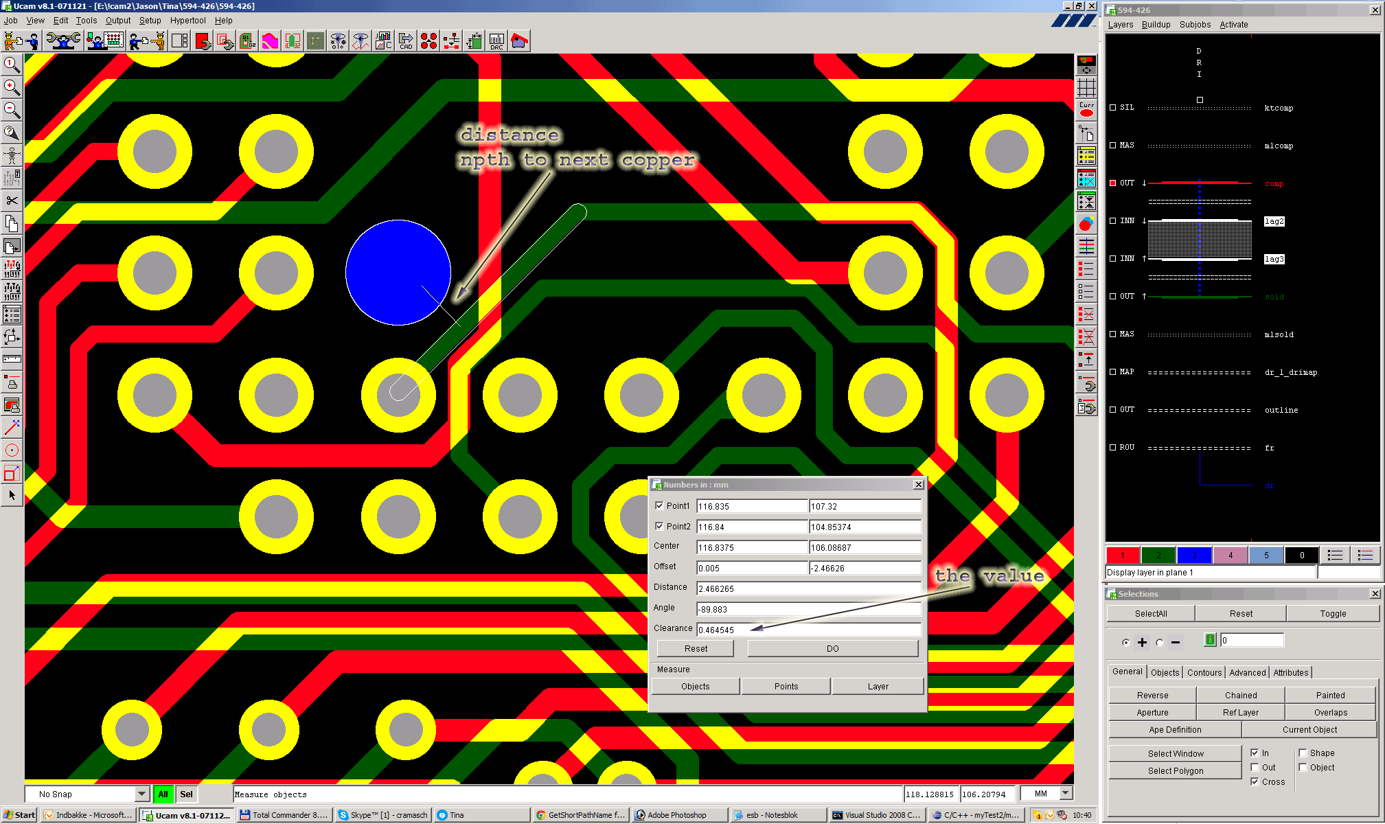
It is a complex program to manipulate drawings in Gerber format, to step them up on a customer panel, and to panelize onto production panel. Finally UCAM is used to output data in many different formats for production.

The reason to learn the process and UCAM was a main part of my job. Further having knowledge about the PCB production process and the UCAM work, I could expand UCAM functionality with pure JAVA. It was not that easy to learn some/many of the included APIs for UCAM, but the results were more then sufficient!

Panel

Why to step the drawings onto customer panels?

One could think, that a PCB as a single board will be used in a device. This is right, but the machines used in the production process would have difficulties when producing one PCB. A small PCB we have to increase in size. So the customer panel will be created.

To ensure the assembly flow the customer panel will get a frame with holes and fiducials in the corners.

Finally the customer panel is stepped again to reach the size of a production panel. Again we add holes and marks, some testing coupons, or even manipulate the copper area on the production panel - all together to get a high-quality product.

What about the production process of the panels?

The panels depending on their build-up are exposed, pressed and drilled, etched and applied with solder mask. In between these steps they are AOI tested on the optical machine. Finally electrical tested, routed out or/and scored, washed and ready to send to the customer.

All these work must be done in the CAM department using some CAM-tools. The CAM has to know the whole production process beginning from the material properties to the electrical test, where the PCB is going to be short/open testet on the machine.

What else do I have to learn for the PCB factory?

To be a good CAM worker it is necessary to learn how the data we prepare in the CAM is handled on the machine, in other words one have to learn to be a machine operator. Very often I helped in the production by plotting films, handling panels on the AOI, electrical test, Silk-screen or even more.

The build-up

Panel Is it a multilayer or is it a double-sided board?
Depending on the type of the PCB we use different approach when preparing the data. For a multilayer it is necessary to create a proper build-up, while the DS PCB do not require it. Further a typical ML board have to be pressed before the drill operation. A pressed ML is like a double-sided board as from this moment on there is not any difference in the production process.

The innerlayers

Panel Innerlayers require in general not that much work as it is the case with outerlayers. However there can be pattern designed on the limit of the feasibility. A special attention must be taken for impedance controlled layers. A wrong build-up, wrong press- parameters or not-allowed modifications on the copper can make the board useless.

The outerlayers

Panel The outer layers are the most visible parts of a PCB where electronics components are soldered. Depending on the current flowing through the board, the PCB designer defines the thickness of the foil used for the outer layers.
The exposing of outer layers is negative, which means that clearences are covered with resist. In the galvanic process the resist-free copper clad is enhanced by galvanic copper and finished by galvanic thin, which is a protection for etchig.

DFM check on innerlayers and outerlayers

Panel This is the most important step in the CAM process as this check ensures about the possibility to produce the PCB-board. If a PCB board has been designed out of capabilities it should be returned to the customer for a redesign. However a company can follow the design and try to produce the board even if they reach capabilities.

The process of step and repeat

A small in size single board is difficult to produce and assembly and will cause a lot of waste. The PCB manufacturer duplicates a single board on to a customer panel. The size of a panel is defined by the customer knowing capabilities of his assembly company. A customer panel is better to test on electrical tester, however testing in production panels is also possible.
A single PCB bigger that 400mm in both directions are not stepped up. This is beacuse of the size of a standard production panel: 457x610mm.

The customer panel

Panel When scoring is used to separate the customer panel it is sometimes usefull to rotate PCBs. This kind of rotation can be a bit challenging for CAM and further for the assembly. Imagine a PCB of a L-shape and the waste when stepping as usual, thus rotation of 180deg better fits the boards on the panel.

Panelizing

When done with the customer panel now is time to panelize into the production panel. Machines in the production require different fiducial marks and holding holes for panels. A frame added for each production panel satisfied every machine and cause possible to produce the boards. Frames are added in the CAM-process by panelizing the boards.
There may be many different panelframes depending on the size of used copper clad for production. Finally when boards are panelized a manual tooling may occur: adding of special fiducials, adding some copper areas, removing copper for V-cut paths.

The production panel

Panel The raster lines and the 15mm copper path around the panel are used for the galvanic line, to ensure a good connection to the electrical clamps. Some extra coupons added on the panel will be used to prepare a microsection of plated vias for a messurement in the laboratory.

The output

not filled out. sorry.

The electrical test

not filled out. sorry.

The AOI (automated optical inspection)

AOI This advanced machine scans a whole production panel in two or three paths, and shows any kind of error to the operator. Honestly there is no need for any electrical test when panels has been watched on this AOI system!

The AOI user interface

AOI_UI Preparing of AOI-data is not a pice of cake and requires some experience. Thus the CAM should not only have knowledge about the ODB++ data but also exprience with operating on the AOI-machine. There are many parameters the operator have to set up, so the algorithm can work efficiently and can show only relevant issues to the operator. Otherwise it will not be easy to find a real issue on the PCB-panel.

The silk-screen machine

Legend printer This nice machine can print any image a user has made data for it. Because of the nozzels, which are very close to the board while printing, the handling on this machine is reserved only for some dedicated stuff.

The silk data

Silk The data have to be prepared for the machine to avoid printing on solder pads. We call it clipping of silk screen with the clearance of min. 150 microns to the pad. Sometimes the clipped silk mask is not usefull anymore. From my point of view the ECAD designer schould pay more attention to the silk screen.

Conclusion

A PCB itself is fascinating, complicated, challenging and difficult with the same. I am proud of my knowledge about the PCB production and proud of my contribution in to the developing of the electronic world. All that would be not possible without the companies I worked for. Thanks go to these companies: HMP, ILFA, elcon and Pri-dana.

All layers at once

Mockup This image demonstrates all layers at once used for production of a multilayer board with 12 copper layers. Having in mind the ready product many of us do not imagine how complicated the board could be.